Patent • #US12098186B1. Provided herein are asymmetric biparatopic neutralizing nanobody-based antibodies which engage SARS-2 spike in at least two independent epitopes. Several biparatopic constructs showed synergy in neutralizing viral infection of cells. Data also showed that single biparatopic constructs are more effective than the combination of the parental monotopic constructs were at...
Search
Muon detectors, systems and methods
Patent • #US10921468B2. A muon detector system capable of determining muon direction and flight trajectory or path is disclosed. The muon detector system includes scintillators for determining muon direction, and an array of muon detectors arranged in orthogonal layers for determining flight trajectory. The system can be used for tomographic and telescopic...
Muon detectors, systems and methods
Patent • #US10451745B1. A muon detector system capable of determining muon direction and flight trajectory or path is disclosed. The muon detector system includes scintillators for determining muon direction, and an array of muon detectors arranged in orthogonal layers for determining flight trajectory. The system can be used for tomographic and telescopic...
Mutli-layered neutron detector
Patent • #US11175417B1. A neutron detector including a plurality of layers of converter material and a plurality of layers of detector material. Each layer of converter material can be immediately adjacent to at least one layer of detector material and each layer of detector material can be immediately adjacent to at least...
Mutually injection locked lasers for enhanced frequency response
Patent • #US8687665B1. Semiconductor light-emitting devices; methods of forming semi-conductor light emitting devices, and methods of operating semi-conductor light emitting devices are provided. A semiconductor light-emitting device includes a first laser section monolithically integrated with a second laser section on a common substrate. Each laser section has a phase section, a gain...
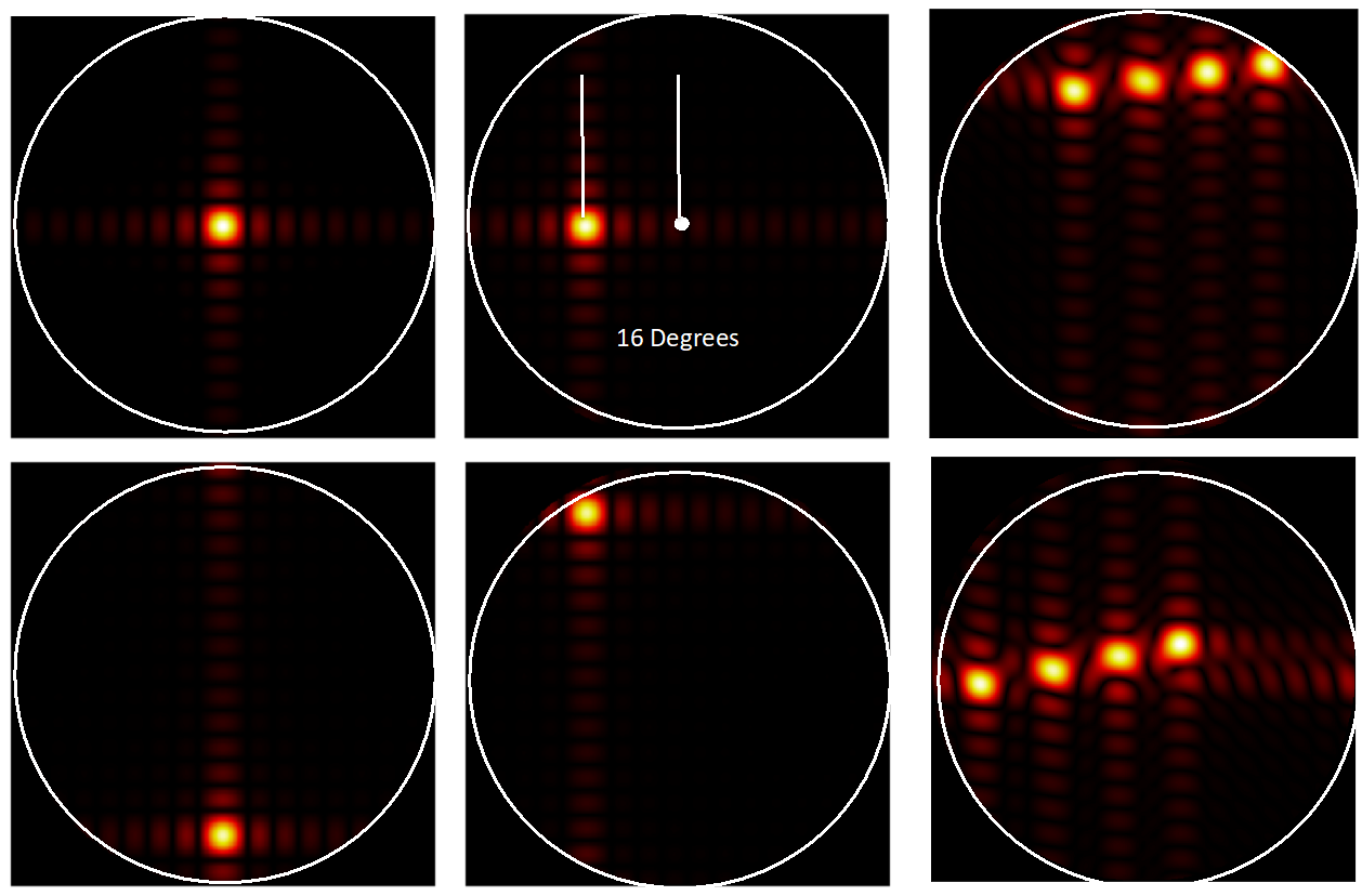
Nanoantenna Phased Array and Transceiver
Featured Opportunity • A scalable, modular architecture and wide-angle array for non-mechanical beamsteering — the basis of chip-scale integrated LIDAR Simulated radiation patterns Integrated photonic LIDAR is a highly complex and challenging integrated photonic technology with potential to enable new capabilities in defense, national security, and commercial applications. Sandia researchers have developed a...
Nanocomposite Anti-Corrosion Coating
Featured Opportunity • A low-cost, environmentally-friendly thin film coating with demonstrated atmospheric corrosion resistance that meets or exceeds conventional coatings 10x as thick Metals across nearly every industry have a need for high performing, low-cost, environmentally-friendly anti-corrosion surface treatments. Films and coatings have long been used to combat corrosion by physically separating metals...
Nanocomposite barrier films for photovoltaic applications
Patent • #US10002983B1. Polymer-clay nanocomposites thin film coatings have improved water vapor and oxygen permeability, in addition to improved corrosion resistance, while retaining high transparency, high electrical resistivity, and excellent fire-retardant properties for use as encapsulants for photovoltaic module assemblies and barrier coatings in other photovoltaic applications.
Nanocomposite conformal corrosion barrier coating
Patent • #US10150873B2. Metals across all industries demand anti-corrosion surface treatments and drive a continual need for high-performing and low-cost coatings. Ordered thin films comprising aligned inorganic platelets dispersed in a polyelectrolyte polymer matrix provide a new class of transparent conformal barrier coatings for protection in corrosive atmospheres. For example, films assembled...
Nanocomposite thermite ink
Patent • #US8048242B1. A nanocomposite thermite ink for use in inkjet, screen, and gravure printing. Embodiments of this invention do not require separation of the fuel and oxidizer constituents prior to application of the ink to the printed substrate.
NanoCoral High Surface Area Platinum Catalysts to Improve Fuel Cell Efficiency
Featured Opportunity • NanoCoralTM produces platinum nanomaterials which can significantly reduce costs and improve the efficiency and durability of hydrogen fuel cells and other renewable energy technologies. NanoCoralTM is an innovative nanotechnology for producing platinum catalysts and offers unique control over the shape, size, porosity, composition, stability, and other functional properties of platinum...
Nanoelectrode array for electrochemical analysis
Patent • #US7625469B1. A nanoelectrode array comprises a plurality of nanoelectrodes wherein the geometric dimensions of the electrode controls the electrochemical response, and the current density is independent of time. By combining a massive array of nanoelectrodes in parallel, the current signal can be amplified while still retaining the beneficial geometric advantages...
Nanoeletromechanical switch and logic circuits formed therefrom
Patent • #US7719318B1. A nanoelectromechanical (NEM) switch is formed on a substrate with a source electrode containing a suspended electrically-conductive beam which is anchored to the substrate at each end. This beam, which can be formed of ruthenium, bows laterally in response to a voltage applied between a pair of gate electrodes...
Nanopatterns by phase separation of patterned mixed polymer monolayers
Patent • #US8652768B1. Micron-size and sub-micron-size patterns on a substrate can direct the self-assembly of surface-bonded mixed polymer brushes to create nanoscale patterns in the phase-separated mixed polymer brush. The larger scale features, or patterns, can be defined by a variety of lithographic techniques, as well as other physical and chemical processes...
Nanoporous Al2O3 as a “Getter” for Volatile Radionuclides into Nanostructured Glass-Ceramic Waste Forms
Featured Opportunity • The first phase of this project is capture and encapsulation which is achieved by using nanoporous alumina to confine gaseous iodine, for example, from fission or waste processing. The captured iodine is then reacted with silver or copper to form precipitates inside the nanopores of the material (the fixation). The...
Nanoporous carbon as an anode material for Li-ion batteries
Patent • #US10784511B1. Nanoporous carbon provides a binderless, three-dimensional form of graphene as an anode material for lithium-ion batteries.
Nanoporous carbon as host material for sodium
Patent • #US11355747B2. Nanoporous carbon can provide a binderless, three-dimensional form of graphene as a host material for sodium-ion batteries or supercapacitors.
Nanoscale bolometer operating near the thermodynamic limit
Patent • #US11788893B1. A nanoscale bolometer for infrared (IR) thermal imaging comprises a subwavelength antenna that provides a specific detectivity approaching a fundamental, thermodynamic limit. The uncooled nanobolometer achieves performance comparable to cooled, high-performance, semiconductor photodetectors, but with significantly reduced size, weight, power, and cost.
Nanoscale Enabled Microinductors for Power Electronics
Featured Opportunity • Scaling of magnetic passive components such as inductors and transformers has not kept pace with advances in high power semiconductor devices employing wide/ultra-wide band gap SiC, GaN, and AlN in terms of size or performance. While higher switching frequencies are enabled by these devices (100 kHz for SiC; 1 MHz...
Nanostructure templating using low temperature atomic layer deposition
Patent • #US8080280B1. Methods are described for making nanostructures that are mechanically, chemically and thermally stable at desired elevated temperatures, from nanostructure templates having a stability temperature that is less than the desired elevated temperature. The methods comprise depositing by atomic layer deposition (ALD) structural layers that are stable at the desired...
Nanostructured metal amides and nitrides for hydrogen storage
Patent • #US10000377B1. Nanostructured metal amides and nitrides are incorporated into nanoporous templates, such as carbon, using liquid ammonia as a solvent/reagent. This leads to unexpected improvements in metal amide nanoconfined hydrogen storage materials. The resulting nanostructured materials may reversibly absorb and desorb large capacities of hydrogen under conditions that are much...
Nanostructured polyelectrolytes for ion-selective membranes
Patent • #US10766005B2. Nanostructured polyelectrolyte bilayers deposited by Layer-by-Layer deposition on nanoporous membranes can be selectively crosslinked to modify the polyelectrolyte charge density and control ionic selectivity independent of ionic conductivity. For example, the polyelectrolyte bilayer can comprise a cationic polymer layer, such as poly(ethyleneimine), and an anionic polymer layer, such as...
Nanowire-templated lateral epitaxial growth of non-polar group III nitrides
Patent • #US7670933B1. A method for growing high quality, nonpolar Group III nitrides using lateral growth from Group III nitride nanowires. The method of nanowire-templated lateral epitaxial growth (NTLEG) employs crystallographically aligned, substantially vertical Group III nitride nanowire arrays grown by metal-catalyzed metal-organic chemical vapor deposition (MOCVD) as templates for the lateral...
Narrow bandwidth detection of vibration signature using fiber lasers
Patent • #US9964431B1. The various technologies presented herein relate to extracting a portion of each pulse in a series of pulses reflected from a target to facilitate determination of a Doppler-shifted frequency for each pulse and, subsequently, a vibration frequency for the series of pulses. Each pulse can have a square-wave configuration,...
Narrow-linewidth single-mode vertical-cavity surface-emitting laser
Patent • #US10892600B1. A coupled-cavity vertical-cavity surface-emitting laser (VCSEL) is disclosed. The coupled-cavity VCSEL includes a passive cavity and an additional distributed Bragg Reflector (DBR) not found in conventional VCSELs, all in a monolithic device. By including these two elements, the photon lifetime may be increased by a factor of approximately ten,...
Results 1101–1125 of 1,895