Piezoelectric Deformable Photonic Devices
A flexible optical platform for phase and amplitude modulation in silicon nitride photonic integrated circuits that offers low optical loss, visible wavelength operation, low power consumption, and performance in cryogenic operating temperatures.
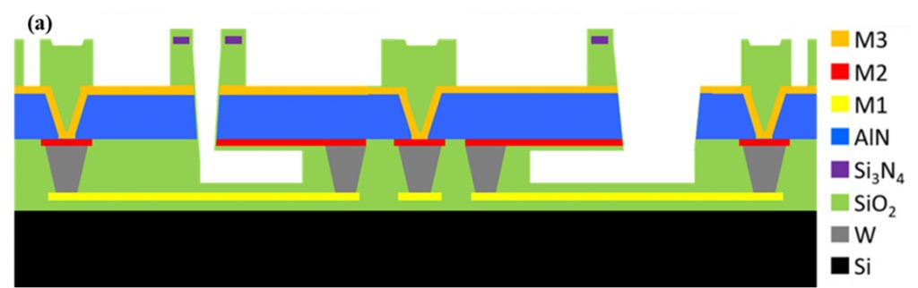
Sandia researchers have developed a flexible optical platform for phase and amplitude modulation in silicon nitride (Si3N4) photonic integrated circuits that offers low optical loss, visible wavelength operation, low power consumption, and performance in cryogenic conditions. The platform, fabricated in a CMOS foundry, enables scalable active photonic integrated circuits for visible wavelengths and the piezoelectric actuation functions without performance degradation down to cryogenic operating temperatures.
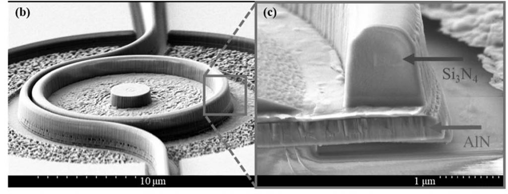
This platform combines low power piezoelectric tuning with the ultra low loss, large bandgap plasma enhanced chemical vapor deposition (PECVD) silicon nitride in a CMOS compatible flow. It utilizes piezo-mechanical coupling with tightly mechanically coupled aluminum nitride (AlN) actuators. The large transparency window of the silicon nitride allows for the design of modulators at most wavelengths of interest in modern photonics. The platform allows for near infrared (NIR) and visible wavelength modulation.
- Maintains optical and piezoelectric performance in cryogenic conditions
- Fabricated in Sandia’s MESA CMOS foundry
- Independent optimization of optical properties and piezoelectric actuation
- Low cost, scalable manufacturing
- Low on-chip power dissipation
- Allows full control of amplitude, phase, and frequency
- Photonic Integrated Circuits (PICs)
- Cryogenic photonic circuit components
- Optical data transmission with visible wavelengths
- Quantum computing
- LiDAR (light detection and ranging)
- Space-based communications
- PICs for neutral atoms, ions, and color vacancy centers
SD# 14944
Published12/3/2019
Last Updated12/20/2019