Additively Manufactured Crystalline Materials
Highly localized, site-specific additive manufacturing of high power conversion efficiency (PCE) crystalline materials for semiconductors and functional devices
Semiconductors are foundational materials that underpin all modern electronic devices ranging from integrated circuits, LEDs, and photovoltaics. One class of crystalline semiconductor material that has gained widespread attention is broadly known as organometallic perovskites. Perovskites have beneficial properties such as high optical gain, long carrier lifetimes, and tunable wavelengths which can enable remarkable power conversion efficiencies (PCE). Despite its promise, there are several challenges to incorporating organometallic perovskite into functional devices, including environmental sensitivity and degradation of physical properties of the crystalline material during processing.
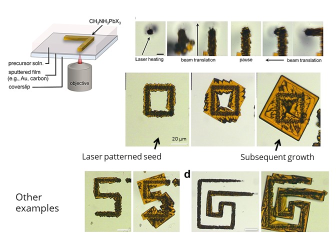
Researchers at Sandia National Laboratories have developed a way to additively manufacture perovskite directly onto devices by thermally inducing crystal growth using a laser direct write approach. This technique addresses the degradation issues that result from exposure to the mixed solvents, photoresists, and etchants found in typical lithographic processes. The ability to direct-write crystalline materials with site-specific accuracy eliminates the need for typical lithographic processes and frees up design space. This technique for highly localized, site-specific additive manufacturing of crystalline materials could greatly enhance the quality and efficiency of high PCE perovskite photovoltaic devices.
- Prevents degradation of crystalline semiconductors when incorporating into functional devices
- Frees up design space due to the ability to direct write with site-specific accuracy
- Flexible placement of the initial crystal growth site supports crystal growth in any pattern
- Manufacturing of crystalline semiconductors for functional electronics, optical, and optoelectronics industries
- Manufacturing of high PCE perovskite photovoltaic devices
SD 13887
Published10/18/2021
Last Updated10/18/2021