Nanoantenna Phased Array and Transceiver
A scalable, modular architecture and wide-angle array for non-mechanical beamsteering — the basis of chip-scale integrated LIDAR
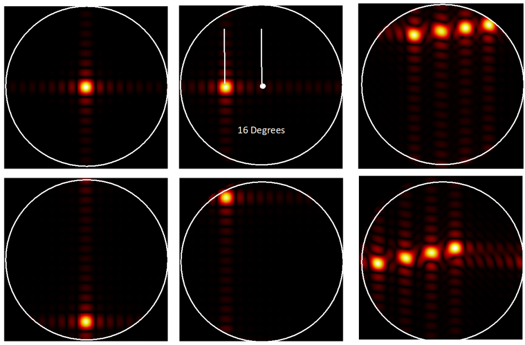
Integrated photonic LIDAR is a highly complex and challenging integrated photonic technology with potential to enable new capabilities in defense, national security, and commercial applications. Sandia researchers have developed a scalable, modular architecture and wide-angle array for nonmechanical electro-optic beam-steering, capable of supporting chip-scale, integrated LIDAR systems.
The device is based on subwavelength spaced metallic nanoantenna fed by Silicon (Si) waveguides. Integrated thermo-optic phase-shifters along the propagation direction allows for subwavelength spacing in the propagation direction, while integrated 2-pi phase shifters on each subwavelength fed waveguide row provide 2D large angle beam steering. This large area array technology is manufactured in a Si CMOS compatible process in which control electronics can be co-integrated, and our phased array technology can be used to form 2D beams with small angular beam size electronically steered over the entire hemisphere. The flexible design of the nanoantenna aperture array allows for tailoring angular beam size and side-lobe suppression which leads to low cross-talk. This technology leverages Sandia’s silicon photonics platform, which encompasses core building blocks of many active and passive photonic devices.
Benefits
- Wide-angle optical beamsteering
- Non-mechanical design enhances reliability and reduces power
- Chipscale, simplified design
- Supports fixed wavelength operation
- Improved beam quality
Applications and Industries
- Automotive
- Aerospace
- Computing and electronics
- Defense
- LIDAR and GIS systems
SD# 12441, 13957
Published3/5/2020
Last Updated3/5/2020